A detailed teardown of NVIDIA’s unreleased TITAN Ada prototype has revealed an unusually complex internal design, highlighting how high-end NVIDIA graphics cards are engineered beyond consumer models., confirming a 90-degree angled PCB layout, 48GB of GDDR6X memory, and a power delivery system capable of handling up to 900 watts.
The teardown was performed by overclocker and hardware expert der8auer on a fully functional prototype, offering the clearest look yet at one of NVIDIA’s most extreme Ada Lovelace-era graphics cards.
Unlike retail GeForce models, the TITAN Ada appears to have been engineered as an uncompromising flagship, combining workstation-class memory capacity with experimental mechanical and electrical design choices that never made it to mass production.
90-Degree PCB Layout Enables Dense Internal Packaging
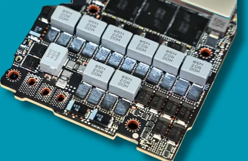
One of the most striking findings is the angled PCB design, where the main board containing the GPU and memory sits parallel to the motherboard, rather than perpendicular like traditional graphics cards. A secondary PCB handles PCIe connectivity and connects to the main board via a flexible interconnect.
This layout allows NVIDIA to pack a very dense PCB while keeping critical components away from the edges of the card. This approach resembles refined design ideas seen in later flagship GPUs, but in the TITAN Ada prototype, it appears more complex and mechanically more demanding.
Full AD102 GPU with 48GB GDDR6X Memory
The teardown confirms that the TITAN Ada prototype is built around a fully enabled AD102 GPU, offering insight into modern GPU architecture decisions at the flagship level, featuring 18,432 CUDA cores. The memory capacity is set at 48GB of GDDR6X, arranged across 24 memory chips, with 12 on the front and 12 on the back of the PCB.
This configuration places the card closer to professional workstation GPUs than consumer GeForce models, which explains why it performed close to, or in some cases better than, existing high-end products during initial benchmark testing.
Quad-Slot Cooler and All-Metal Construction

Cooling is handled by a quad-slot, triple-fan cooler with an all-metal exterior. The heatsink dominates the card’s internal volume, with very little of the PCB visible from the side. Multiple integrated heat pipes are built directly into the structural components, spreading heat throughout the entire assembly before transferring it to the main cooling array.
This design prioritizes thermal stability under extreme power loads over compactness, resulting in a significantly larger and heavier card.
900W-Ready Power Delivery with Dual 12V Connectors
Power delivery is one of the most unique aspects of the TITAN Ada prototype. Instead of standard-looking power sockets on the PCB, the card utilizes dual 12V-2×6 connectors that draw power through solid copper conductors integrated into the cooler itself.
NVIDIA paired the prototype with a custom adapter that converts six 8-pin connectors into two 12V-2×6 inputs, supporting power levels up to 900W. Sense pins and contact pads are integrated directly into the cooling structure, reducing reliance on traditional cabling but significantly increasing manufacturing complexity.
This approach differs from both the RTX 4090 Ti prototype and subsequent retail designs, highlighting the experimental nature of the TITAN Ada project. Why the TITAN Ada Never Became a Retail Product
While the teardown showcases impressive engineering, it also helps explain why the TITAN Ada was never commercially launched. The card’s extreme power requirements, high production costs, and overlap with professional RTX workstation GPUs would have made it difficult to position within NVIDIA’s product stack.
The assembly alone would have been time-consuming and expensive, especially at low production volumes. According to the report, even reassembling the prototype took over an hour, illustrating how impractical this design would have been for mass manufacturing.
A Glimpse into NVIDIA’s Most Ambitious GPU Engineering

The TITAN Ada prototype is a rare example of NVIDIA pushing the boundaries of GPU engineering without commercial constraints. Many of its ideas, such as the angled PCB, distributed power delivery, and aggressive thermal design, have influenced later flagship products, even though the card itself never reached consumers.
Consequently, the teardown provides valuable insight into how NVIDIA experiments internally before refining concepts for mainstream and professional GPUs.
Source: VideoCardz, based on the der8auer teardown


